


Research Progress
Significant Progress in Efficient Pure-Red Perovskite Light-Emitting Diodes
The Changchun Institute of Applied Chemistry, Chinese Academy of Sciences (CIAC, CAS) has achieved significant progress in the efficient luminescence study of pure-red perovskite light-emitting diodes (PeLEDs). The research team led by Qin Chuanjiang proposed a novel ligand engineering strategy that, by modulating crystallization kinetics, enabled in situ construction of highly oriented quasi-two-dimensional perovskite nanosheets in thin films, achieving highly horizontal orientation of optical transition dipole moments (TDMs). This approach raised the external quantum efficiency (EQE) of 635 nm pure-red PeLEDs to 31.2% for the first time. The related research results were published in the prestigious international optics journal Light: Science & Applications under the title "In-situ formation of oriented perovskite nanosheets with tailored optical dipoles enabling >30% EQE in pure-red LEDs."
Low-dimensional perovskite materials, with their quantum confinement effects and anisotropic optical properties, represent a highly promising pathway for overcoming luminescence efficiency limits. Previous studies have shown that traditional perovskite nanosheet fabrication strategies employ a "synthesize-then-film" approach, where synthesized colloidal perovskite nanosheets can exhibit near-100% luminescent quantum yields in suspension. However, integrating these solution-phase nanosheets into functional films not only makes precise crystal orientation control difficult but also renders the energy barrier for forming intact nanosheets within films extremely high due to ligand-induced lattice distortion and interlayer mismatch. Therefore, conventional methods typically yield only randomly oriented nanocrystals, leading to increased defects and dramatically reduced efficiency. Overcoming this thermodynamic and kinetic limitation to achieve ordered construction of intact nanosheet structures within films has become an urgent challenge in the field.
To address these challenges, the research team proposed an in situ nanosheet fabrication strategy, selecting 2-naphthylmethylamine (2-NMA) as the ligand for quasi-two-dimensional perovskites. By introducing the 2-NMA ligand with smaller terminal steric hindrance and stronger interlayer π-π interactions, they precisely and substantially reduced the energy barrier for nanosheet formation to below 0 eV. This thermodynamic and kinetic optimization enabled the induction of in situ crystal seed growth during room-temperature spin coating, successfully transforming the originally disordered isotropic film into a structurally intact nanosheet film with face-on orientation. The in situ constructed perovskite nanosheet film achieved highly horizontal TDM orientation (86%) and significantly enhanced interlayer electronic coupling, enabling carrier mobility comparable to pure three-dimensional perovskites. Based on this core in situ nanosheet fabrication approach, the team successfully fabricated 635 nm pure-red PeLEDs with an external quantum efficiency as high as 31.2% and peak luminance improved to 13,400 cd m⁻², with overall performance at the leading edge. Furthermore, this strategy successfully achieved large-area uniform luminescent devices with an emitting area of 12 cm², validating its tremendous potential for practical display applications.
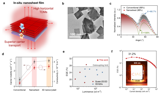
Figure 1. Schematic illustration of in situ nanosheet construction, microscopic morphology, nanosheet film characterization, and electroluminescent device performance with large-area fabrication demonstration.
This study, through an innovative ligand engineering strategy, successfully overcame the bottleneck of disordered crystal orientation in solution-processed perovskite films, not only constructing highly oriented quasi-two-dimensional nanosheets in situ within films but also, through this core approach, breaking through 30% EQE for pure-red PeLEDs for the first time. This work provides an effective means for surpassing light extraction efficiency limits in luminescent devices and opens new avenues for designing next-generation efficient display technologies, lasers, and solution-processed semiconductor devices for integrated photonics.
The research results are published in Light: Science & Applications:
https://doi.org/10.1038/s41377-026-02184-x


 Address: No. 5625 Renmin Street Changchun City Jilin Province P.R. China
 Tel: 86-0431-85687300